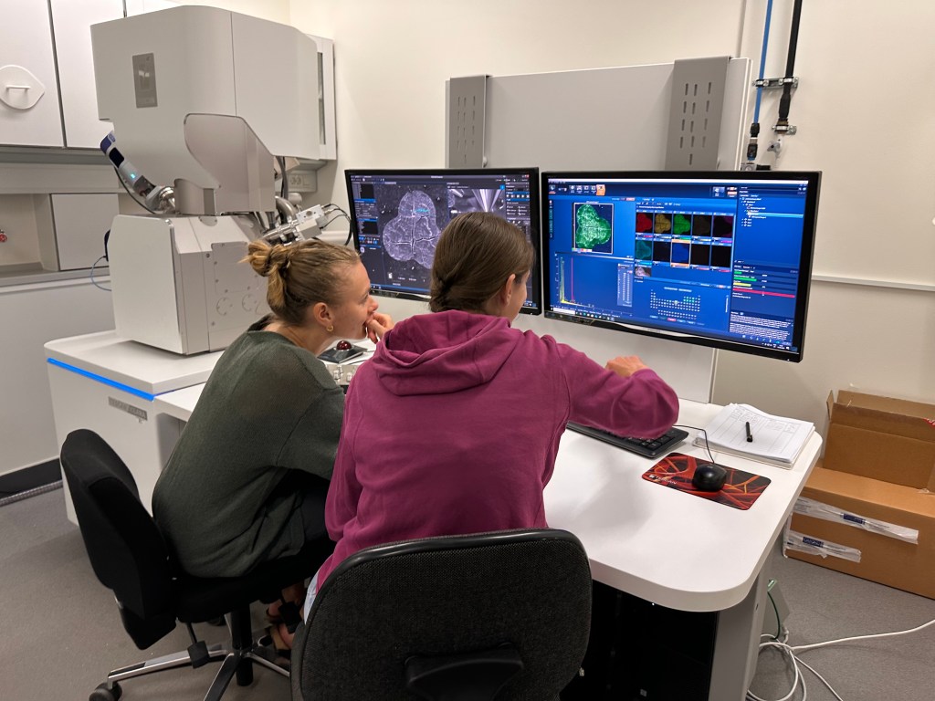
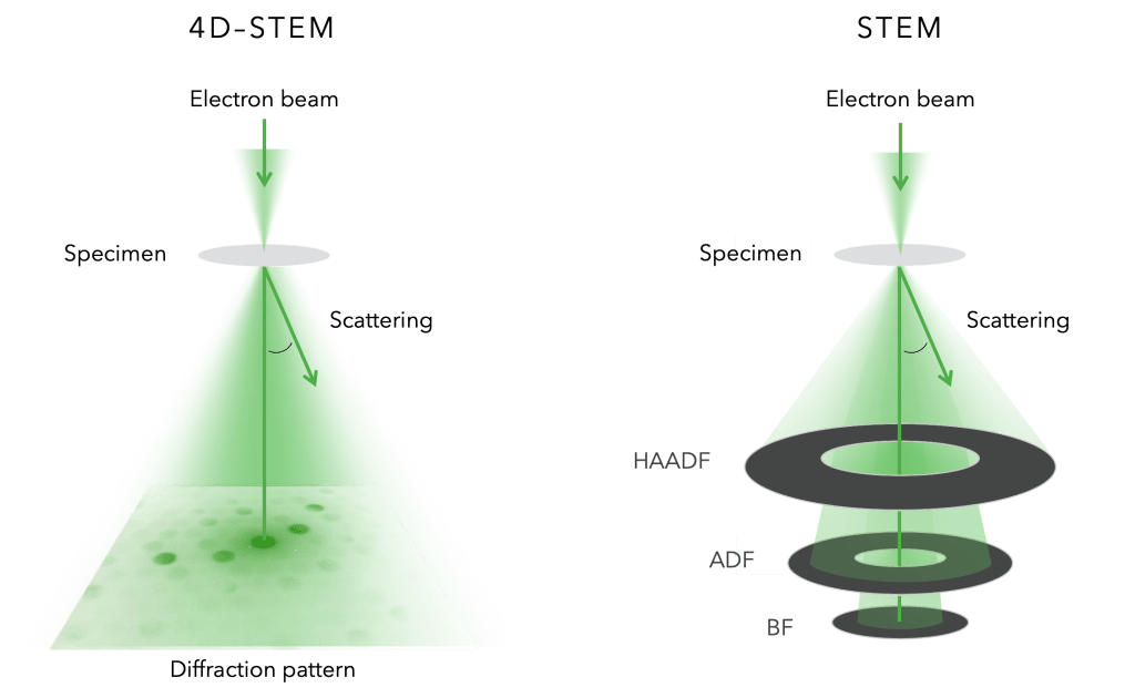
4D-Scanning Transmission Electron Microscopy (4D-STEM)
Utilizing a state-of-the-art direct electron detector, we can acquire full diffraction patterns rather than integrated intensities while scanning in STEM. This approach, known as 4D-STEM, enables advanced data processing to extract rich structural information from materials at the nanoscale.
We apply 4D-STEM to a wide range of materials and research questions. This includes phase and orientation mapping of next-generation battery cathodes, strain mapping in guanine nanocrystals, and multiscale defect analysis in gold alloy nanoparticles. Our group also develops advanced analysis methods, such as local symmetry mapping of short-range order, structural similarity metrics in crystalline regions, and innovative denoising techniques for diffraction data. In addition, we perform time-resolved 4D-STEM to investigate material degradation processes and dynamic phase transitions between ordered and disordered states.
Energy Dispersive X-ray Spectroscopy (EDX)
When a sample is bombarded with high-energy electrons, core-shell electrons from some atoms are ejected. As electrons from higher energy levels fall into these electron vacancies, they release excess energy in the form of X-rays with element-specific energies. Energy dispersive X-ray spectroscopy (EDX) detects these X-rays to determine the elemental composition of the sample.
We use EDX in both the SEM and the STEM not only to identify which elements are present, but also to map their spatial distribution. By scanning the electron beam across the sample, we can visualize where specific elements are located. This allows us to investigate whether catalytic materials are uniformly distributed on their supports or if elements in multi-metallic nanoparticles are well-mixed or segregated. These spatial insights are crucial for understanding material performance and behavior. A key scientific question is how thoroughly elements are mixed at the nanoscale, and to what extent we can experimentally confirm this mixing. To support this analysis, we’ve developed a custom Python script, eeee, that streamlines EDX data processing, making it easier to extract, visualize, and interpret elemental maps and spectra.
Powder X-ray Diffraction (PXRD)
Powder X-ray diffraction (PXRD) is used to characterize the crystalline structure of materials. When a beam of monochromatic X-rays interacts with a polycrystalline sample, the atomic planes within crystalline domains diffract the radiation at specific angles, resulting in a characteristic diffraction pattern. This pattern acts as a structural fingerprint, allowing phases to be identified and structural order to be assessed.
Because PXRD averages over many randomly oriented crystallites, it provides information on the long-range, ensemble-averaged structure of a material. Well-defined diffraction peaks indicate crystalline order, while broad or diffuse features signal small crystallite sizes, structural disorder, or amorphous content. By analyzing peak positions, intensities, and widths, PXRD can be used to determine lattice parameters, identify crystalline phases, and monitor structural changes e.g. during synthesis, heat treatment, or operation.
Total Scattering – Pair Distribution Function (PDF) Analysis
The pair distribution function (PDF) is a method used for both short- and long-range order structural characterization. The PDF describes the probability of finding atoms at a certain distance from each other, thereby making it possible to extract information about the interatomic distances, coordination number, domain size, and crystallinity.
As it is possible to obtain structural information for even very disordered and amorphous materials, the technique is very useful for studying a variety of materials. Not only where the traditional scattering methods such as powder X-ray diffraction (PXRD) fail to provide the necessary structural information, but also to analyze disordered domains within a crystalline material. This makes the technique powerful for revealing and investigating structures which would otherwise have been left unexplored.
PDF is a technique which can be utilized with both X-rays and electrons.
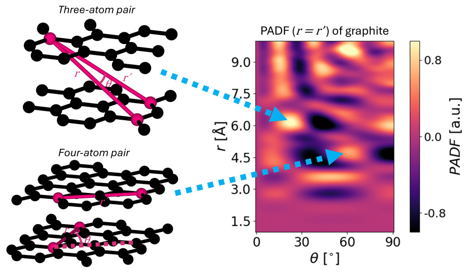
Pair-Angle Distribution Function (PADF)
The pair-angle distribution function (PADF) characterizes atomic arrangements in materials by correlating two atomic pair distances (r, r’) with the angle (θ) between the atomic pairs. This makes PADF a rich source of structural information, capturing both atomic distances – similar to the pair distribution function (PDF) – and angular arrangements. Consequently, it is more sensitive to structural differences than PDF.
Because of its ability to detect angular arrangements that other techniques often cannot access, PADF is particularly useful for studying materials where traditional scattering methods or physical property measurements suggest structural differences but fail to precisely identify them. For example, PADF enables a more detailed analysis of disordered materials, such as disordered carbons and glass fibers. Additionally, it can be applied to more crystalline materials that exhibit significant stacking faults, as PADF is highly sensitive to stacking disorder. This capability makes it a powerful tool for revealing subtle structural complexities that might otherwise remain undetected.
X-ray Absorption Spectroscopy (XAS)
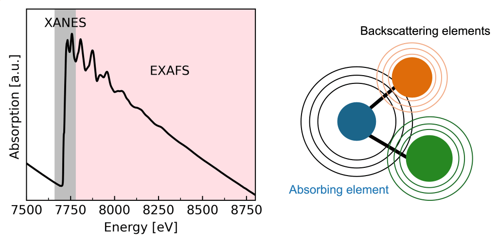
X-ray absorption spectroscopy (XAS) allows us to zoom in on the local environment of a specific element. By scanning the energy of incoming X-rays across the absorption edge of an element, we observe how strongly the sample absorbs X-rays as the photons gain just enough energy to excite core electrons.
At the edge, a sharp increase in absorption, the edge jump, marks the energy required to eject a core electron. The region around this edge form the X-ray absorption near-edge structure (XANES), typically spanning about -20 to +50 eV relative to the edge. XANES provides insight into oxidation state, coordination geometry, and electronic structure of the absorbing atom.
Farther above the edge, oscillations in the absorption signal make up the extended X-ray absorption fine structure (EXAFS). These oscillations arise from interference between the outgoing photoelectron from the absorbing element and waves scattered by neighboring atoms, allowing EXAFS to reveal bond lengths, coordination numbers, and local disorder.
Together, XANES and EXAFS give a powerful, element-specific picture of a material’s local structure, even when the sample is amorphous, disordered, or part of a complex mixture. To perform these experiments we have to go synchrotron facilities.
X-Ray Tomography
Just as having two eyes gives us depth perception, imaging a sample from multiple angles allows us to reconstruct its three-dimensional structure. In X-ray tomography, we collect a series of X-ray absorption images, called projections, from different angles. These projections form a sinogram, which is mathematically related to the sample through the Radon transform and can be reconstructed using algorithms based on its inverse.
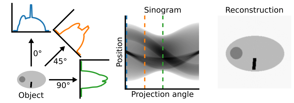
X-ray absorption tomography produces a 3D volume that reflects the electron density distribution within the sample. This volumetric data can indirectly suggest elemental composition and reveal structural features such as pores, cracks, or inclusions. We perform these measurements in-house using an advanced X-ray microscope, the Xradia 620 Versa, which offers high-resolution imaging capabilities. For more specialized contrast mechanisms, such as X-ray diffraction tomography, we go to synchrotron facilities such as DanMAX at MAX IV. These techniques allow us to map crystallographic phases and gain deeper insights into the material’s internal structure. Together, these tools provide a powerful platform for non-destructive, multi-scale characterization of complex materials.
Focused Ion Beam – Scanning Electron Microscopy (FIB-SEM)
To obtain nano- to atomic scale structural information on materials utilizing TEM techniques, a thin electron transparent sample is needed. FIB-SEM combines a focused ion beam for precise milling and material modification with a scanning electron microscope for high-resolution imaging. The two-beam instrument is optimal for sample preparation as the electron beam can be used to continuously guide and monitor the FIB milling process by scanning the beam across the area of interest as the ion beam mills out a section of the sample. Milling removes sample atoms and enables a thin section of the sample of interest to be created for further investigation.
Local Symmetry Analysis
Local symmetry analysis is a data analysis strategy that employs angular correlation analysis to extract symmetry information from the local crystal structure. Central to this approach is the use of the angular autocorrelation function, which allows quantifying the angular symmetry elements in local electron diffraction patterns, which reflects the symmetry characteristics of the underlying crystal structure.
This method is particularly valuable for studying amorphous and disordered materials, which lack long-range order and are challenging to characterize using conventional diffraction techniques alone. By highlighting recurring local symmetries, it aids in identifying and classifying structural patterns within the materials. For example, we have successfully applied local symmetry analysis to investigate structural features in disordered carbons and metallic glasses. In addition, local symmetry analysis serves as a powerful tool for reducing the dimensionality of complex 4D-STEM datasets.
Simulations
Simulations are computer-generated experiments that help us explore how complex systems behave under controlled, virtual conditions. They allow us to produce large amounts of synthetic data, which we use to develop and test our analysis techniques, often faster and more cost-effective than conducting physical experiments.
In the DISORDER group, we study materials and phenomena where experimental data can be difficult to interpret or obtain in sufficient detail. Simulations provide us with datasets where we know the exact underlying structure, serving as a “ground truth” for validating our analysis methods. By applying our techniques to this simulated data, we can assess their accuracy and refine them before using them on real experimental results. Recently, we’ve generated several hundred gigabytes of virtual 4D-STEM datasets of gold particles using the py_multislice Python package by Hamish Brown, which we are planning to use for testing defect detection methods.
Instruments
Talos STEM
- Field emission gun (X-FEG), energy spread 0.8 eV
- STEM resolution of 0.16 nm, HRTEM resolution of 0.12 nm
- Fully aligned for operation at 80 kV and 200 kV acceleration voltages
- HAADF, 2x ADF and BF detectors for STEM imaging
- Ceta 16M pixel CMOS camera
- Quantum Detectors quad-chip (512 x 512) MerlinEM direct electron detector
- Super-X G2 EDS, 0.9 sr solid angle
- Velox software v2.16
- Gatan GIF with EELS with 2k CCD (??)
Holders:
- Single tilt holder ± 35 alpha tilt
- Double tilt holder ± 35 alpha tilt and ± 30 beta tilt
- Tomography holder ± 70 alpha tilt
- Gatan heating holder up to ~900 °C
Clara SEM
- Schottky field emission source
- Operational at 0.5 – 30 kV acceleration voltages
- Probe currents from 2 pA to 400 nA, continuously adjustable
- Resolution of 0.8 nm @ 30 kV in STEM, and 1.2 nm @ 1 kV with (beam deceleration)
- Motorized, 5-axis goniometer stage
Detectors:
- Everhart-Thornley chamber detector
- In-column Energy-Filtered Multidetector
- In-column axial SE/BSE detector
- 4Q BSE detector
- 2nd generation CMOS EBSD detector
- STEM-in-SEM detector
- Oxford Ultim Max 40mm2 EDS detector with AztecLive Standard Software